8.4.2. Diode Characteristic Curve
#r# This example shows how to simulate and plot the characteristic curve of a diode.
#r#
#r# Theory
#r# ------

#r# A diode is a semiconductor device made of a PN junction which is a sandwich of two doped silicon
#r# layers.

#f# tikz('diode.tex', width=500)

#r# Before two explains the purpose of the silicon doping.  We will give a quick and simplified look
#r# on the atomic world.  An atom is made of the same number of protons and electrons, this number
#r# is so called Z and characterise the atom.  Each electron is coupled to the proton's kernel by
#r# the electromagnetic interaction, but with different levels of energy.  The reason is due to the
#r# fact each electron screens each other.  There is thus some electrons which are strongly coupled
#r# and other ones which are weakly coupled, so called valence's electrons.  An atom is a neutral
#r# object when we observe it at a large distance, but when the pressure and temperature of the
#r# environment match some conditions, the weakly coupled electrons can be shared with atoms in the
#r# neighbourhood and create the electromagnetic interaction between atoms which make the cohesion
#r# of the matter.

#r#
#r# Depending on the weakness of the electrons, an atom can be an insulated material or a conductor.
#r# Semiconductors are between them.

#r#
#r# The doping consists to diffuse a small quantities of atoms with a larger or smaller number of
#r# valence electron in a silicon layer.  Since a silicon atom has four valence electrons, we use
#r# atoms having 3 or 5 valence electrons for the doping.  A doping using a larger number of valence
#r# electrons is called N for negative, and P respectively.  In a silicon lattice doped with atoms
#r# having a larger number of valence electrons, the additional electrons do not participate to the
#r# lattice cohesion and are weakly coupled to the atoms.  The conductivity is thus improved.  In
#r# other hands, a silicon lattice doped with atoms having a smaller number of valence electrons,
#r# some electrons are missing for the lattice cohesion.  These missing electrons are called holes
#r# since the P doping atoms will catch free electrons so as to normalise the lattice cohesion.

#r#
#r# When we make a sandwich of P and N doped silicon layers, the weak electrons of the N layer
#r# diffuse to the P layer until an equilibrium state is achieved.  Indeed this diffusion creates a
#r# depletion region which acts as a barrier to the electrons, since a P doping atom becomes negative
#r# (anion) when it catches an electron and reciprocally a N doping atom becomes positive (cation)
#r# when it lost an electron.  The depletion region is thus a kind of capacitor.

#r#
#r# The volume of the depletion region can be changed by applying a tension across the PN junction.
#r# If the tension between the PN junction is negative then the depletion region is enlarged, and
#r# only a very small current can flow through the junction due to the thermal agitation.  But if we
#r# apply a positive tension, the depletion region is pressurised, and if it reaches a threshold, an
#r# electron flow will be able to pass through the junction.

#r#
#r# A PN junction can thus only conduct a current from the anode to the cathode and only if a
#r# minimal bias tension is applied across it.

#r#
#r# However if a large enough inverse tension is applied to the junction then the electrostatic
#r# force will become sufficiently large enough to pull off electrons across the junction and the
#r# current will flow from the cathode to the anode. This effect is called breakdown.

#r#
#r# Simulation
#r# ----------

####################################################################################################

import numpy as np
import matplotlib.pyplot as plt
import matplotlib.ticker as ticker

####################################################################################################

import PySpice.Logging.Logging as Logging
logger = Logging.setup_logging()

####################################################################################################

from PySpice.Doc.ExampleTools import find_libraries
from PySpice import SpiceLibrary, Circuit, Simulator
from PySpice.Unit import *
from PySpice.Physics.SemiConductor import ShockleyDiode

####################################################################################################

libraries_path = find_libraries()
spice_library = SpiceLibrary(libraries_path)

####################################################################################################

#r# For this purpose, we use the common high-speed diode 1N4148.  The diode is driven by a variable
#r# voltage source through a limiting current resistance.

#f# circuit_macros('diode-characteristic-curve-circuit.m4')

circuit = Circuit('Diode Characteristic Curve')

circuit.include(spice_library['1N4148'])

circuit.V('input', 'in', circuit.gnd, 10@u_V)
circuit.R(1, 'in', 'out', 1@u_Ω) # not required for simulation
circuit.X('D1', '1N4148', 'out', circuit.gnd)

#r# We simulate the circuit at these temperatures: 0, 25 and 100 °C.

# Fixme: Xyce ???
temperatures = [0, 25, 100]@u_Degree
analyses = {}
simulator = Simulator.factory()
for temperature in temperatures:
    simulation = simulator.simulation(circuit, temperature=temperature, nominal_temperature=temperature)
    analysis = simulation.dc(Vinput=slice(-2, 5, .01))
    analyses[float(temperature)] = analysis

####################################################################################################

#r# We plot the characteristic curve and compare it to the Shockley diode model:
#r#
#r# .. math::
#r#
#r#     I_d = I_s \left( e^{\frac{V_d}{n V_T}} - 1 \right)
#r#
#r# where :math:`V_T = \frac{k T}{q}`
#r#
#r# In order to scale the reverse biased region, we have to do some hack with Matplotlib.
#r#

silicon_forward_voltage_threshold = .7

shockley_diode = ShockleyDiode(Is=4e-9, degree=25)

def two_scales_tick_formatter(value, position):
    if value >= 0:
        return '{} mA'.format(value)
    else:
        return '{} nA'.format(value/100)
formatter = ticker.FuncFormatter(two_scales_tick_formatter)

figure, (ax1, ax2) = plt.subplots(2, figsize=(20, 10))

ax1.set_title('1N4148 Characteristic Curve ')
ax1.set_xlabel('Voltage [V]')
ax1.set_ylabel('Current')
ax1.grid()
ax1.set_xlim(-2, 2)
ax1.axvspan(-2, 0, facecolor='green', alpha=.2)
ax1.axvspan(0, silicon_forward_voltage_threshold, facecolor='blue', alpha=.1)
ax1.axvspan(silicon_forward_voltage_threshold, 2, facecolor='blue', alpha=.2)
ax1.set_ylim(-500, 750) # Fixme: round
ax1.yaxis.set_major_formatter(formatter)
Vd = analyses[25].out
# compute scale for reverse and forward region
forward_region = Vd >= 0@u_V
reverse_region = np.invert(forward_region)
scale =  reverse_region*1e11 + forward_region*1e3
#?# check temperature
for temperature in temperatures:
    analysis = analyses[float(temperature)]
    ax1.plot(Vd, - analysis.Vinput * scale)
ax1.plot(Vd, shockley_diode.I(Vd) * scale, 'black')
ax1.legend(['@ {} °C'.format(temperature)
            for temperature in temperatures] + ['Shockley Diode Model Is = 4 nA'],
           loc=(.02,.8))
ax1.axvline(x=0, color='black')
ax1.axhline(y=0, color='black')
ax1.axvline(x=silicon_forward_voltage_threshold, color='red')
ax1.text(-1, -100, 'Reverse Biased Region', ha='center', va='center')
ax1.text( 1, -100, 'Forward Biased Region', ha='center', va='center')

#r# Now we compute and plot the static and dynamic resistance.
#r#
#r# .. math::
#r#
#r#   \frac{d I_d}{d V_d} = \frac{1}{n V_T}(I_d + I_s)
#r#
#r# .. math::
#r#
#r#   r_d = \frac{d V_d}{d I_d} \approx \frac{n V_T}{I_d}

ax2.set_title('Resistance @ 25 °C')
ax2.grid()
ax2.set_xlim(-2, 3)
ax2.axvspan(-2, 0, facecolor='green', alpha=.2)
ax2.axvspan(0, silicon_forward_voltage_threshold, facecolor='blue', alpha=.1)
ax2.axvspan(silicon_forward_voltage_threshold, 3, facecolor='blue', alpha=.2)
analysis = analyses[25]
static_resistance = -analysis.out / analysis.Vinput
dynamic_resistance = np.diff(-analysis.out) / np.diff(analysis.Vinput)
ax2.semilogy(analysis.out, static_resistance, base=10)
ax2.semilogy(analysis.out[10:-1], dynamic_resistance[10:], base=10)
ax2.axvline(x=0, color='black')
ax2.axvline(x=silicon_forward_voltage_threshold, color='red')
ax2.axhline(y=1, color='red')
ax2.text(-1.5, 1.1, 'R limitation = 1 Ω', color='red')
ax2.legend(['{} Resistance'.format(x) for x in ('Static', 'Dynamic')], loc=(.05,.2))
ax2.set_xlabel('Voltage [V]')
ax2.set_ylabel('Resistance [Ω]')

plt.tight_layout()
plt.show()

#f# save_figure('figure', 'diode-characteristic-curve.png')

#r# We observe the forward voltage threshold increase with the temperature.
#?# #r# Indeed the thermal agitation overcome the electron flow.
This example shows how to simulate and plot the characteristic curve of a diode.
8.4.2.1. Theory
A diode is a semiconductor device made of a PN junction which is a sandwich of two doped silicon layers.

Before two explains the purpose of the silicon doping. We will give a quick and simplified look on the atomic world. An atom is made of the same number of protons and electrons, this number is so called Z and characterise the atom. Each electron is coupled to the proton’s kernel by the electromagnetic interaction, but with different levels of energy. The reason is due to the fact each electron screens each other. There is thus some electrons which are strongly coupled and other ones which are weakly coupled, so called valence’s electrons. An atom is a neutral object when we observe it at a large distance, but when the pressure and temperature of the environment match some conditions, the weakly coupled electrons can be shared with atoms in the neighbourhood and create the electromagnetic interaction between atoms which make the cohesion of the matter.
Depending on the weakness of the electrons, an atom can be an insulated material or a conductor. Semiconductors are between them.
The doping consists to diffuse a small quantities of atoms with a larger or smaller number of valence electron in a silicon layer. Since a silicon atom has four valence electrons, we use atoms having 3 or 5 valence electrons for the doping. A doping using a larger number of valence electrons is called N for negative, and P respectively. In a silicon lattice doped with atoms having a larger number of valence electrons, the additional electrons do not participate to the lattice cohesion and are weakly coupled to the atoms. The conductivity is thus improved. In other hands, a silicon lattice doped with atoms having a smaller number of valence electrons, some electrons are missing for the lattice cohesion. These missing electrons are called holes since the P doping atoms will catch free electrons so as to normalise the lattice cohesion.
When we make a sandwich of P and N doped silicon layers, the weak electrons of the N layer diffuse to the P layer until an equilibrium state is achieved. Indeed this diffusion creates a depletion region which acts as a barrier to the electrons, since a P doping atom becomes negative (anion) when it catches an electron and reciprocally a N doping atom becomes positive (cation) when it lost an electron. The depletion region is thus a kind of capacitor.
The volume of the depletion region can be changed by applying a tension across the PN junction. If the tension between the PN junction is negative then the depletion region is enlarged, and only a very small current can flow through the junction due to the thermal agitation. But if we apply a positive tension, the depletion region is pressurised, and if it reaches a threshold, an electron flow will be able to pass through the junction.
A PN junction can thus only conduct a current from the anode to the cathode and only if a minimal bias tension is applied across it.
However if a large enough inverse tension is applied to the junction then the electrostatic force will become sufficiently large enough to pull off electrons across the junction and the current will flow from the cathode to the anode. This effect is called breakdown.
8.4.2.2. Simulation
import numpy as np
import matplotlib.pyplot as plt
import matplotlib.ticker as ticker


import PySpice.Logging.Logging as Logging
logger = Logging.setup_logging()


from PySpice.Doc.ExampleTools import find_libraries
from PySpice import SpiceLibrary, Circuit, Simulator
from PySpice.Unit import *
from PySpice.Physics.SemiConductor import ShockleyDiode


libraries_path = find_libraries()
spice_library = SpiceLibrary(libraries_path)
For this purpose, we use the common high-speed diode 1N4148. The diode is driven by a variable voltage source through a limiting current resistance.
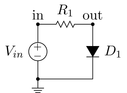
circuit = Circuit('Diode Characteristic Curve')

circuit.include(spice_library['1N4148'])

circuit.V('input', 'in', circuit.gnd, 10@u_V)
circuit.R(1, 'in', 'out', 1@u_Ω) # not required for simulation
circuit.X('D1', '1N4148', 'out', circuit.gnd)
We simulate the circuit at these temperatures: 0, 25 and 100 °C.
# Fixme: Xyce ???
temperatures = [0, 25, 100]@u_Degree
analyses = {}
simulator = Simulator.factory()
for temperature in temperatures:
    simulation = simulator.simulation(circuit, temperature=temperature, nominal_temperature=temperature)
    analysis = simulation.dc(Vinput=slice(-2, 5, .01))
    analyses[float(temperature)] = analysis
We plot the characteristic curve and compare it to the Shockley diode model:
where \(V_T = \frac{k T}{q}\)
In order to scale the reverse biased region, we have to do some hack with Matplotlib.
silicon_forward_voltage_threshold = .7

shockley_diode = ShockleyDiode(Is=4e-9, degree=25)

def two_scales_tick_formatter(value, position):
    if value >= 0:
        return '{} mA'.format(value)
    else:
        return '{} nA'.format(value/100)
formatter = ticker.FuncFormatter(two_scales_tick_formatter)

figure, (ax1, ax2) = plt.subplots(2, figsize=(20, 10))

ax1.set_title('1N4148 Characteristic Curve ')
ax1.set_xlabel('Voltage [V]')
ax1.set_ylabel('Current')
ax1.grid()
ax1.set_xlim(-2, 2)
ax1.axvspan(-2, 0, facecolor='green', alpha=.2)
ax1.axvspan(0, silicon_forward_voltage_threshold, facecolor='blue', alpha=.1)
ax1.axvspan(silicon_forward_voltage_threshold, 2, facecolor='blue', alpha=.2)
ax1.set_ylim(-500, 750) # Fixme: round
ax1.yaxis.set_major_formatter(formatter)
Vd = analyses[25].out
# compute scale for reverse and forward region
forward_region = Vd >= 0@u_V
reverse_region = np.invert(forward_region)
scale =  reverse_region*1e11 + forward_region*1e3
for temperature in temperatures:
    analysis = analyses[float(temperature)]
    ax1.plot(Vd, - analysis.Vinput * scale)
ax1.plot(Vd, shockley_diode.I(Vd) * scale, 'black')
ax1.legend(['@ {} °C'.format(temperature)
            for temperature in temperatures] + ['Shockley Diode Model Is = 4 nA'],
           loc=(.02,.8))
ax1.axvline(x=0, color='black')
ax1.axhline(y=0, color='black')
ax1.axvline(x=silicon_forward_voltage_threshold, color='red')
ax1.text(-1, -100, 'Reverse Biased Region', ha='center', va='center')
ax1.text( 1, -100, 'Forward Biased Region', ha='center', va='center')
Now we compute and plot the static and dynamic resistance.
ax2.set_title('Resistance @ 25 °C')
ax2.grid()
ax2.set_xlim(-2, 3)
ax2.axvspan(-2, 0, facecolor='green', alpha=.2)
ax2.axvspan(0, silicon_forward_voltage_threshold, facecolor='blue', alpha=.1)
ax2.axvspan(silicon_forward_voltage_threshold, 3, facecolor='blue', alpha=.2)
analysis = analyses[25]
static_resistance = -analysis.out / analysis.Vinput
dynamic_resistance = np.diff(-analysis.out) / np.diff(analysis.Vinput)
ax2.semilogy(analysis.out, static_resistance, basey=10)
ax2.semilogy(analysis.out[10:-1], dynamic_resistance[10:], basey=10)
ax2.axvline(x=0, color='black')
ax2.axvline(x=silicon_forward_voltage_threshold, color='red')
ax2.axhline(y=1, color='red')
ax2.text(-1.5, 1.1, 'R limitation = 1 Ω', color='red')
ax2.legend(['{} Resistance'.format(x) for x in ('Static', 'Dynamic')], loc=(.05,.2))
ax2.set_xlabel('Voltage [V]')
ax2.set_ylabel('Resistance [Ω]')

plt.tight_layout()
plt.show()
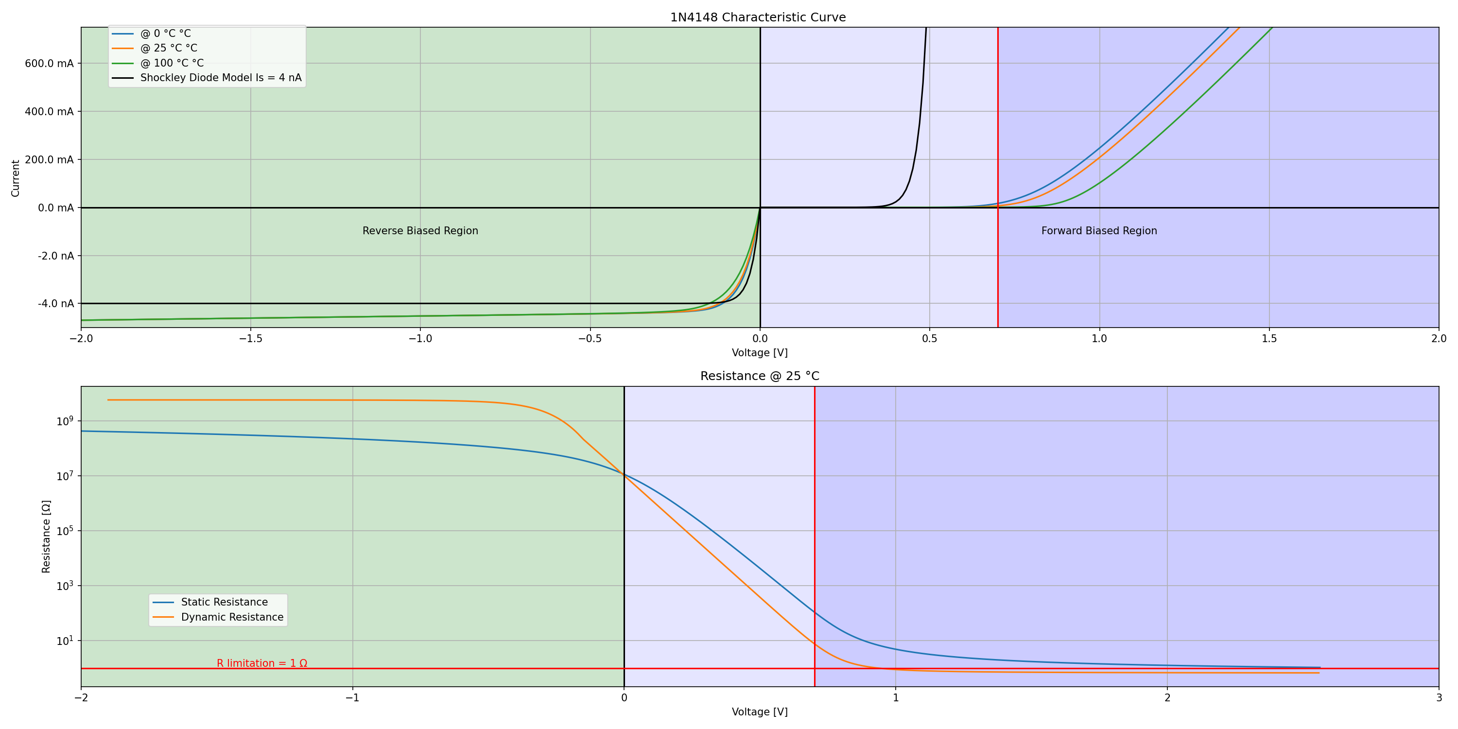
We observe the forward voltage threshold increase with the temperature.